Vacuum magnetron sputtering station "Kepler 450"

The unit is designed for spraying single-layer and multi-layer coatings by magnetron sputtering. Argon is used as a sputter gas.

Установка

The magnetron sputtering station Kepler 450 has the following advantages:

• The maximum possible number of loaded substrates in one spraying cycle - 4.

• The ability to spray multilayer coatings from two or three different materials in one working cycle has been implemented.

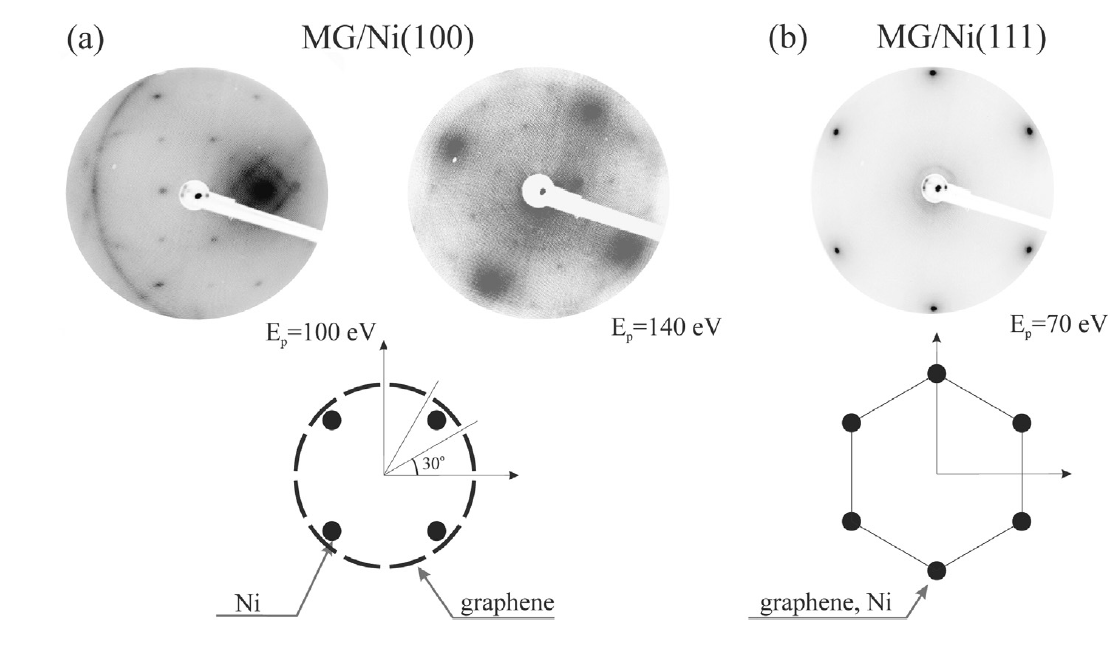
• The magnetron sputtering process can be carried out both in constant current mode and in radio frequency (RF) mode.

• One magnetron operates in DC mode only, while the other two magnetrons operate in two modes: DC mode and RF mode.

• The supply of up to two reactive gases at the same time has been implemented.

• The system deposition implements the possibility of ion etching of samples using a KLAN-103M ion source.

• The possibility of heating the substrates has been implemented.

• It is possible to use targets of two different diameters using appropriate magnetic systems, which allows slow deposition of thin films (from 1 nm) on a small system, or deposition of thicker films (up to tens of microns) on the main system at a high speed.

• The thickness of the sprayed coating is measured using quartz sensors installed inside the chamber.

Target parameters

• Large target - target diameter from 87 mm to 91 mm, target thickness from 0.5 mm to 8 mm;
• Small target - target diameter from 50 mm to 52 mm, target thickness from 0.5 mm to 4 mm.

Year of issue: 2019

Passport

Manual

Technical description of the ion source KLAN-103M

Patents

A EAPO(Eurasia Patent Organisation) and FIIP (Federal Institute of Industrial Property, Russia) patents for the invention "A method for obtaining monolayer silicene" were issued.

Authors: RC PMSI employees Zhizhin E.V. и Pudikov D.А., Solid State Electronics department employee Komolov A.S.

Patent holder: Saint Petersburg University

A FIIP (Federal Institute of Industrial Property, Russia) patent for the utility model "A device for producing organic thin-film coatings in vacuum" was issued.

Authors: RC PMSI employees Zhizhin E.V. и Pudikov D.А., Solid State Electronics department employee Komolov A.S.

Patent holder: Saint Petersburg University

A FIIP (Federal Institute of Industrial Property, Russia) patent for the invention "A device for producing structured graphene" was issued.

Authors: RC PMSI employees Zhizhin E.V. и Pudikov D.А.

Patent holder: Saint Petersburg University

The state registration certificate of a computer program was issued "Program for recording photoelectronic spectra" (XPS spectra).

Authors: SPBU researchers Rybkin A.G., Usachov D.Yu. and RC FMIP members of staff Zhizhin E.V. и Pudikov D.А.

Patent holder: Saint Petersburg University

The state registration certificate of a computer program was issued "Program for controlling the operating mode of a vacuum ultraviolet radiation source" (VUV-Valve).

Authors: SPBU researchers Vilkov O.Yu., Usachov D.Yu. and RC FMIP members of staff Zhizhin E.V. и Pudikov D.А.

Patent holder: Saint Petersburg University

A FIIP (Federal Institute of Industrial Property, Russia) patent for the invention "The method for producing graphene at low temperatures" was issued.

Authors: RC PMSI employees Zhizhin E.V. и Pudikov D.А.

Patent holder: Saint Petersburg University

A Eurasian patent for the invention "The method for producing graphene at low temperatures" was issued.

Inventors: RC PMSI employees Zhizhin E.V. и Pudikov D.А.

Patent holder: Saint Petersburg University

Methods of synthesis and diagnostics

  1. 1. Technique of the surface cleaning of monocrystals of refractory and transition metals up to atomic cleanliness during realization of R & D

    This technique describes the operations of cleaning of monocrystals of refractory metals by high-temperature "flash" and monocrystals of transition metals by ion etching in ultrahigh vacuum conditions.

  2. 2. Technique of permanent deposition of different metals with a continuous control of the thickness of deposited layers during realization of R & D

    This technique is based on a experimental registration of manifestations of quantum size effects in thin layers on the surface of metal monocrystals continuously for increasing the thickness of the deposited film, starting from submonolayer thicknesses, with using the method of photoelectron spectroscopy with angular resolution (ARPES). The film thickness can be measured with an accuracy of a few tenths of a monolayer and controlled based on the observed spectrum of the quantum electronic states by analysing their energy and quantity. This technique can be used in the manufacture of precision quantum nanoelectronic devices and new nanostructured materials.

  3. 3. Technique of testing of the crystal structure of monocrystal surfaces and their orientation for researches by method of photoelectron spectroscopy with angular resolution by high-resolved details of LEED patterns during realization of R & D

    LEED is widely used to study of the crystal structure of single crystal surfaces in ultrahigh vacuum conditions. Information about the structure of the surface is obtained by analyzing the elastically scattered electrons by the crystal, and this leads to the conclusion about perfection of the crystal structure of the sample, the orientation of the crystallographic axes in space. This information is necessary for the proper orientation it in the right direction for further crystallographic study of dispersion of the energy bands along the preferred directions of the surface Brillouin zone with high symmetry by photoelectron spectroscopy with angular resolution (ARPES). This technique reduces the time required for characterization and orientation of single crystal surface or low-dimensional structures formed on its surface.

  4. 4. The technique of measuring of the dispersion of the energy band structure and occupied and unoccupied state by the photoelectron spectra with high angular and energy resolution during realization of R & D

    Using this technique provides a unique opportunity to receive information about the electronic energy structure and the corresponding dispersion dependences of the electronic states of the valence band of the objects. These possibilities become particularly important in the study of the processes of the formation and analysis of the electronic properties of nanostructured low-dimensional objects of 2D- and 1D-type, where there is a substantial modification of the electronic structure of the valence states due to quantum size effects. Such modification allows to create objects with a fundamentally new type of electronic structure (which can be modified in a controlled manner) and, consequently, leads to radically new electronic properties of created objects. Therefore, it is very important to have the opportunity to study and control the electronic structure and the dispersion of the electronic states in the required direction of the Brillouin zone, where there are dimensional constraints of the wave functions of nanosystem.

  5. 5. Technique of elemental and chemical analysis of solids by the method of photoelectron spectroscopy of core levels

    Photoelectron spectroscopy allows to determine  binding energy of core levels in solids. Each element has its own set of energies of core levels (alike a "fingerprint"), herewith energy of core levels, corresponding to different elements, quite well energetically separated. This technique allows to identify various elements by the photoelectron spectra, i.e., get information about elemental composition of investigated system. By defining energy peaks in the photoelectron spectra it is possible to get information not only about atoms of which elements are located at the solid surface, but also in which are they chemical state. The formation of chemical bonds between atoms of a solid body, accompanied by a redistribution of the electron density, can lead to a change in the energy of electrons that will, certainly, appear in the change of kinetic energy of photoelectrons.

  6. 6. Technique of the raster depth profiling

    Study of the distribution of elements over the depth is carried out using the technique of a raster ion profiling. Essence of a technique is the following: investigated surface alternately etched with argon ions and study by XPS. The result is a set of photoelectron spectra at different time of surface etching. Etching time determines the thickness of sputtered layer. For example, calibration using an atomic force microscope provides a quantitative relation between depth and time of etching.

  7. 7. Technique of synthesis of graphene by chemical vapor deposition

    This technique allows to synthesize one-domain graphene on surface of thin monocrystal layers of nickel and cobalt.
     

Research methods

  1. 1. X-ray photoelectron spectroscopy (XPS) and X-Ray photoelectron imaging (XPi)

    The method of photoelectron spectroscopy is a modern method of investigation of occupied electronic states in solids. It is based on the phenomenon of the photoelectric effect: electron in a solid is optically excited by a photon to the unoccupied state. Photoelectron spectroscopy of core levels enables to obtain quantitative information about elemental and chemical composition of the surface area of ​​the samples. Method of elemental mapping of surface is used for study elemental and chemical composition of samples with lateral resolution, the implementation of this method is possible due to the presence of special microchannel plate, which allows to analyze the emitted photoelectrons from a solid body with a spatial resolution.
     

    Escalab 250Xi

    Nanolab (without imaging)

    Univer-M (without imaging)


  2. 2. Spin and angle resolved photoelectron spectroscopy (SARPES) of valence band

     
    The method of photoelectron spectroscopy with angular resolution is widely used for measuring of dispersions and symmetry of electron energy bands of solid state.
     

    Escalab 250Xi (Ultraviolet PES without angle and spin resolution)

    Nanolab

    Univer-M


  3. 3. Low energy electron difraction (LEED) 

     
    Method of LEED provides information about single crystal structure of the sample surface.


    Graphene LEED on: (a) Ni(100), Ep = 100 eV, (b) Ni(111), Ep=110 eV.


    Escalab 250Xi

    Nanolab

    Univer-M


  4. 4. Auger electron spectroscopy (AES) and scanning auger electron mapping (SAM)

     
    The origin of Auger electron spectroscopy (AES) is measurement of energy and intensity of Auger electrons emitted from the sample surface when it is bombarded with a beam of electrons. An important feature of the Auger electron spectroscopy is its sensitivity to chemical state of analyzed elements on the surface. The chemical state of elements of the sample affects the shape and position of features of the spectrum of the Auger electrons.


    Auger maps (C KLL and Ni LMM lines) and SEM image (50×50 μm) of the sample after heating of system Ni/ВОПГ up to 310°C


    Escalab 250Xi

    Univer-M


  5. 5. Scanning electron microscopy (SEM)

     
    The method allows to obtain an image of the sample surface by scanning with focused electron beam (up to 95 nm and 10 keV) with simultaneous recording of low-energy secondary electrons, excited by this beam.
     

    Escalab 250Xi

    Univer-M


  6. 6. Ion scattering spectroscopy (ISS)

     
    Ion scattering spectroscopy (ISS) is a technique in which a beam of primary ions is scattered by a surface. The kinetic energy of scattered ions is measured. Energy losses depend on the relative masses of the surface atoms and ions, thereby measured spectrum contains information about elemental composition. 
     

    Escalab 250Xi


  7. 7. Reflected electron energy loss spectroscopy (REELS)

     
    Electron energy-loss spectroscopy is a kind of electronic spectroscopy, when investigated surface irradiated by electrons with a narrow range of energies, and losses of energy of inelastically scattered electrons are recorded. Distribution of electron energies carries information about energy loss due to excitation of vibrational states, plasmons, deep levels and interband transitions.

    Escalab 250Xi


  8. 8. Scanning tunneling microscopy (STM) and scanning tunneling spectroscopy (STS) 

     
    These methods allow to obtain images of surface with atomic resolution, energy spectra of occupied and unoccupied states, distribution of work function and local density of states with high lateral resolution.
     

    STM image of graphene-containing system surface, recieved by constant tunnel current: (а) graphene, synthesized on Ni-substrate; (b) gold, dusted on graphene-Ni system; (c) system after heating up to 310°C. Right peace shows model, wich demonstrates Moire pattern, arising because of overlapping of a gold monolayer and a graphene lattice.

    Nanolab


  9. 9. Atomic force microscopy (AFM) (contact and non-contact modes)


    Nanolab


  10. 10. Reflectron time-of-flight mass spectrometry (TOF-MS)

    Time-of-flight mass spectrometry (TOFMS) is a method of mass spectrometry in which an ion's mass-to-charge ratio is determined via a time measurement. Using a reflector leads to a significant increase in resolution time-of-flight devices in compare with linear increases spectrometers and to an increase of mass determination accuracy. Selection of ionization source depends on substance state before ionization. Ionization is possible by electron impact or by laser radiation (photoionization).

    Univer-М


  11. 11. Thermal desorption spectroscopy (TDS)

    Essense of the method is measuring composition of desorbed gas from sample heated in a vacuum in dependence on the temperature. The method allows to determine binding energy of adsorbed atoms and molecules (or activation energy of desorption), amount of surface coverage by adsorbed substances, order of kinetics of adsorption process.

    Univer-М


Certification

Course "Bases of operation, storage and transportation of ballons":

Course "Bases of design and safe operation of vessels, working under pressure":

Course "Bases of safe operation of compressed-air installations":

Patent "Graphene spin filter" (registered 6 May 2016 year):


"Week of high technologies" (1-4 March 2016):


Analytical and testing equipment Shimadzu seminar (20-22 October 2015):


Course "Automation of chemical warehouse based on software 1C: Bookkeeping of state establishment":


Training on the photoelectron spectrometer Phoenexs and Russian-German Photoemission Station in Helmhotz-Zentrum Berlin (Germany, 2013):


Training on the hemispherical analyzer VG Scienta R4000 with 3D spin Mott detector in Dresden University of Technology (Germany, 2012):


3rd International School on Surface Science "Technologies and Measurements on Atomic Scale" (Sochi, 23-29 September 2013):


Training regarding operation of Multifunctional UHV system for surface investigation using XPS/UPS/ARPES (Poland, 5-6 November 2012):

2nd International School on Surface Science "Technologies and Measurements on Atomic Scale" (Sochi, 1-7 October 2012):