Welcome to the page of resource center "Physical methods of surface investigation" (Saint Petersburg University Research park)!
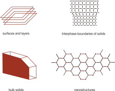
The purpose of the Resource center (RC PMSI) is to carry out research work in an ultrahigh vacuum, dedicated to the study of surface nanostructures and composite materials, to the analysis of the local atomic structure, morphology, and the features of the electronic energy and spin structure. The main experimental methods implemented in the RC are: Auger electron spectroscopy, X-ray and ultraviolet photoelectron spectroscopy, as well as superhigh-vacuum tunneling and atomic force microscopy.
On this site you will find complete information about our equipment, methods of surface investigation and the results of the users of the RC.
| News | |
| 24.08.2022 | With the participation of the Resource Center "Physical Methods of Surface Investigation", the 300th anniversary article was published in a periodical (see section "Publications"). |
| 09.08.2022 | From the Baikonur cosmodrome, 16 small spacecraft of the Space-π educational project were launched as an associated payload during the launch of a commercial foreign satellite. Among the launched small spacecraft is the "Geoscan-Edelweiss" satellite, the navigation system of which was created using components modified under the agreement between Geoscan LLC and St. Petersburg State University. To do this, work was carried out on the deposition of coatings of a given shape in the resource centers of the Research Park of St. Petersburg State University: "Physical methods of surface investigation" (Kepler 450 magnetron sputtering facility) and "Nanostructuring of photoactive materials" (photolithography).
Detailed information is available at Geoscan website |
| 02.08.2022 | Employees of the resource center "Physical methods of surface investigation" Zhizhin E.V. and Pudikov D.A. together with an employee of the Department of Solid State Electronics Komolov A.S. developed a technology for producing silicene monolayer using the equipment of the resource center. This material was obtained in practice for the first time at St. Petersburg State University. Silicene is a silicon analog of graphene: it is a material that has the same crystal structure, but consists of silicon atoms. Recently, theoretical work has begun to appear showing the similarity of these materials in terms of the electronic structure parameters that made graphene so popular: both have a Dirac cone of electronic states at the K-point of the Brillouin zone, and the charge transfer is carried out by massless fermions. However, due to the instability of the silicon atom monolayer, very little is known about successful methods for the production of silicene. According to the technology, the synthesis is carried out by the method of molecular-beam epitaxy on the Ag(111)/W(110) system. The resulting silicene has rather large sizes of individual domains (up to 100 nm). For the developed technology, the authors have been issued a Russian and Eurasian patent (see section"Patents"). |
| Manipulation | Core research areas | Objects of interest |
|
Control of electronic properties Control of geometric structure Control of processes |
Photoactive materials Thermoelectric materials Catalysts Biomaterials Nanoelectronics and spintronics Graphene and topological insulators Magnetism of nanostructures |
 |

 English (UK)
  Русский (РФ)